Description
Description
The Omega/Theta X-ray diffractometer is a fully automated vertical three axes diffractometer for orientation determination for various crystals using Omega-Scan and Theta-Scan methods and rocking curve measurements. The large and spacious design can accommodate samples and sample holders up to 450 mm in length and up to 30 kg weight.
Highlights:
-
Sample size up to 450 mm
-
Advanced, user-friendly software
-
Automated rocking-curve measurement
-
Low energy consumption and operating costs
-
Convenient sample handling and easy to operate
-
Angular resolution of the diffractometer: 0.1 arc sec.
-
Appropriate for production quality control and research
-
Ultra-fast crystal orientation measurement using Omega-scan method
-
Fully automated complete lattice orientation measurement of single crystals
Application
Orientation mapping of crystalline surfaces
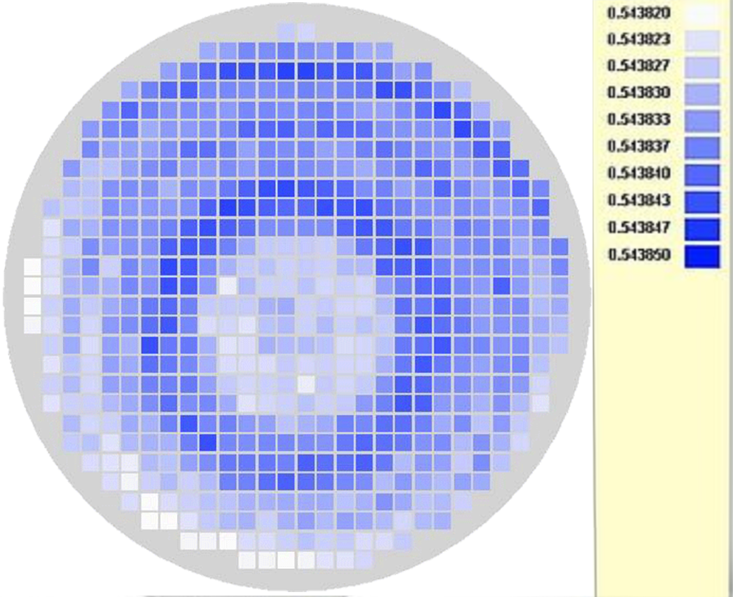
Even in a single crystal, the crystal orientation can exhibit small changes over the surface, which result from internal strains caused by lattice defects. Orderly grown thin films can also have an interesting in-plane orientation distribution. Mapping a surface requires a lot of measurements. Here the Omega Scan method can offer its advantage in speed. The picture shows an orientation map measured on a (Si, Ge) solid solution wafer. The maximum orientation difference is 0.03°. Concentric circles follow the growth rings of the crystal.

Automatic wafer sorting
To gain the high performance that is expected from a semiconductor, every wafer shall be tested. With its high speed and precision, the Omega-scan method is best suited for fully automated in-line solutions of XRD. This includes characterization of the surface tilt vector and an in-plane direction, for instance the perpendicular of the flat as well as automated detection of flat- or notch plus their measures.
For all established wafer materials and orientations, Omega Scan solutions are available. The most common material is quartz, where the combination with mapping comes in handy. The high-quality areas of the wafer are identified prior to cutting blanks.
 More detail about Atomic Solutions Sdn Bhd


 Malaysia