Look Small But Unbelievable Performance Like Floor Model SEM
Description:
The Thermo Scientific Phenom Pharos G2 FEG-SEM brings field emission SEM to your tabletop. The Phenom Pharos G2 FEG-SEM will outperform many floor-standing SEMs in terms of image quality, while offering a vastly better user experience. For academic and industrial laboratories that so far did not consider SEM a realistic option, the Phenom Pharos G2 FEG-SEM makes FEG performance accessible thanks to its attractive form factor and short training required. Blazing fast sample loading means fast sample exchange, which means higher productivity. Unlike other SEMs, which end up being fully booked, the Phenom Pharos G2 FEG-SEM performs imaging and analysis jobs so quickly that it serves well as a walk-up tool.
The new Phenom Pharos G2 FEG-SEM expands its acceleration voltage range down to 1 kV, to better accommodate insulating and beam-sensitive samples, and up to 20 kV, with a resolution of 2.0 nm that reveals the finest details.Options include a secondary electron detector (SED) and/or energy-dispersive X-ray detector (EDX/EDS), live colour element identification, mixed imaging, along with sophisticated analytical software
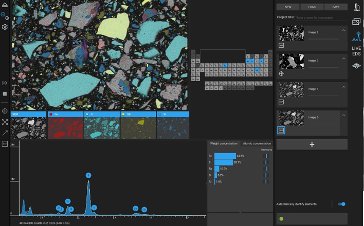
The optional EDS detection suite on the Phenom Pharos G2 Desktop FEG-SEM offers comprehensive element analysis with a few clicks andwithin a few seconds.
Features:
The fastest higher-resolution desktop SEM with less than 40sec imaging.
1 - 20KV Acceralation voltages
2.0nm Resolution
Field Emission Gun (FEG) source desktop SEM
Up to 2,000,000x Magnification
Intergrated Charge Reduction Mode
Optional with STEM Detector
Maps 3 with large area EDS mapping, Correlation study with other type of tools.
Phase Analysis
LIVE Colour EDS for element identification & mapping
Application:
Scientists and researchers in academia and industry who want to create higher-quality products, improve specifications, discover new applications, and develop new materials will require access to the smallest length scales.
The morphology of nanoparticles, small defects in thin films, insulating materials, or materials sensitive to high-kV electron beams can be adequately studied only by using a field emission SEM. A field emission electron source provides a stable, high-brightness beam, and field emission tips usually last longer than a year, meaning you will not have regular downtime for source exchange.
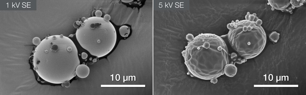
Sensitive materials require gentle conditions. With an acceleration voltage down to 1 kV, the Phenom Pharos G2 Desktop FEG-SEM images beam-sensitive samples without sample coating or other sample preparation. Left: pharmaceutical powder, imaged without damage at 1 kV. Right: the same sample imaged at 5 kV, with damage, illustrating the need for low-kV imaging.
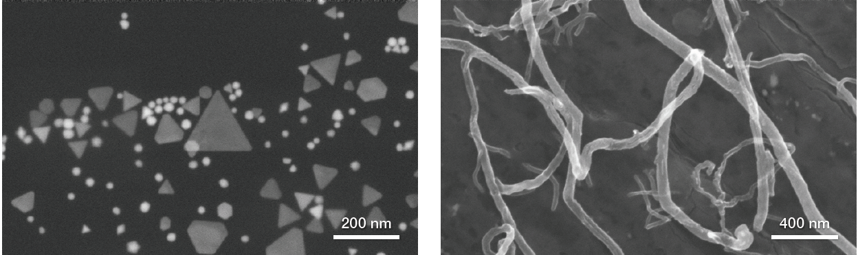
Nanomaterial characterization becomes truly accessible with the Phenom Pharos G2 Desktop FEG-SEM. Left: gold nanoparticles, backscatter electron image. Right: carbon nanotubes, secondary electron image.
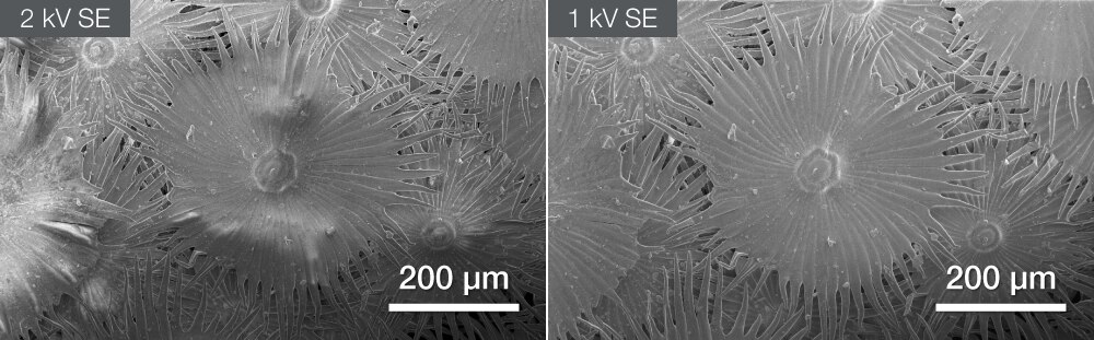
Uncoated insulators, such as this sea shell, can only be properly imaged at low acceleration voltage. At 2 kV (left image), significant charging artefacts can still be observed. At 1 kV (right image), those artifacts have disappeared.


